Building Your Factory on a Megasite 🗺️🏭🏗️
Site selection, contracting a specialized design firm, and procuring building materials and equipment all require technology to build a factory on a megasite.
The modern-day factory has transformed into a high-tech hub, the buildings are as high-tech as the companies they house. It's a smart environment that seamlessly integrates Industry 4.0 technologies, creating a space where data, connectivity, and intelligence drive efficiency and quality.
Before the fanfare of a ribbon-cutting ceremony, a significant amount of groundwork must be laid. The process begins with the crucial task of site selection, where factors such as infrastructure, accessibility, and environmental impact are considered. Next, a design firm is contracted to create a blueprint that aligns with the factory's operational needs and sustainability goals. Finally, the procurement of building materials and construction equipment is undertaken, setting the stage for the actual construction. Each of these steps is integral to transforming a plot of land into a fully functioning, high-tech factory.
Who Selects the Megasite? 🗺️
The journey to a high-tech factory begins with site selection and evaluation. This process, often initiated by governments and navigated by advisory firms, can shape the future of industrial development.
Governments offer incentives like grants, tax breaks, and favorable zoning laws to attract businesses, fostering industrial growth and job creation.
Advisory firms like KBC Advisors, instrumental in scaling Amazon's industrial real estate footprint, employ a data-driven approach to identify optimal sites for their clients. They consider factors like physical attributes, transportation access, expansion potential, and the local labor market.
When governments and advisory firms align their efforts, they can stimulate industry clustering dynamics. This synergy can lead to increased innovation, a larger pool of skilled workers (and potentially cause a shortage), and shared infrastructure. Thus, while the site selection process can be complex, it's a pivotal first step toward creating a modern, sustainable factory.
Semiconductor Clustering Dynamics Are at Play in Greater Phoenix, Arizona, USA
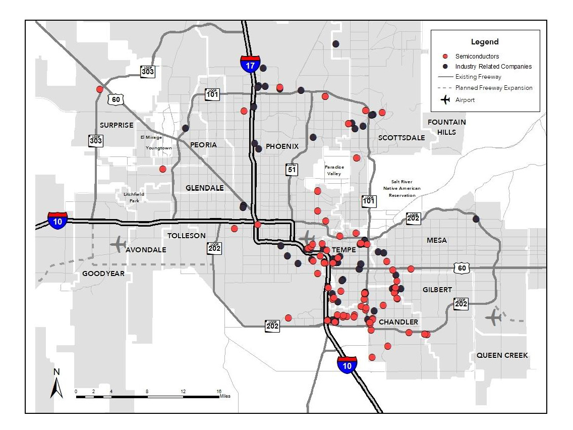
Phoenix, Arizona, is fast becoming the ‘capital’ for semiconductor companies, reminiscent of Detroit's automotive industry boom a century ago. Economists David A. Price and Zhu Wang's analysis of the U.S. automotive industry in its first 75 years highlights the importance of inter-industry spillovers (benefits from proximity to firms in related industries) in establishing an industry center. In the case of the automotive industry revolution, it was correlated to locales with carriage and wagon manufacturing. With Phoenix and the semiconductor industry, it could be related to its history in transistors dating back to Motorola in 1949. The presence of semiconductors and related industry companies in the Greater Phoenix region is prominent as shown in the map below.

Other areas, like Syracuse, New York are hoping their advantages for semiconductor fabs in available land, access to clean power, and abundance of water will “trigger the creation of a cluster of companies that result in a flourishing of new innovation.” The semiconductor industry structure (OEMs and supply chain) is much different than automotive so perhaps that may come true. Regardless of which location is selected, the factory must be well designed for the manufacturing processes it houses.
Check out the semiconductor clusters emerging in Phoenix and Syracuse in our Factory Boom map. Also explore the new sector clusters that are materializing in batteries, electronics, and automotive.
Which Firms Design and Build a Factory? 🏭📐
In North America, few design and engineering firms have the capabilities to build a leading-edge factory. The Engineering News-Record (ENR) tracks the chaotic construction industry by performing annual surveys of its key segments including manufacturing. Topping the list of manufacturing design firms include Jacobs, Wood, Ghafari Associates, and Exyte. More on each of them below.
Each firm is developing and applying new technology to better manage risk and deliver cost-effective solutions for their OEM clients. And although we can 3D print a house, we cannot yet scale up the technology to meet the requirements of a large-scale manufacturing facility.
Additionally, each sector has special considerations to take into account when constructing their facilities. Semiconductor fabs, for example, require expertise in the creation of cleanrooms. The expertise is so crucial to be done correctly the first time that TSMC has brought in foreign workers to Arizona to address the specialized needs in “cleanroom setup, pipeline installation, mechanical and electrical systems for chip plants, and other specialized areas.” The aforementioned firms are at the top of the ENR list not only due to their general competency but also their unique expertise in the hot sectors of semiconductors, batteries, and automotive.
Jacobs Solutions (Advanced Manufacturing)
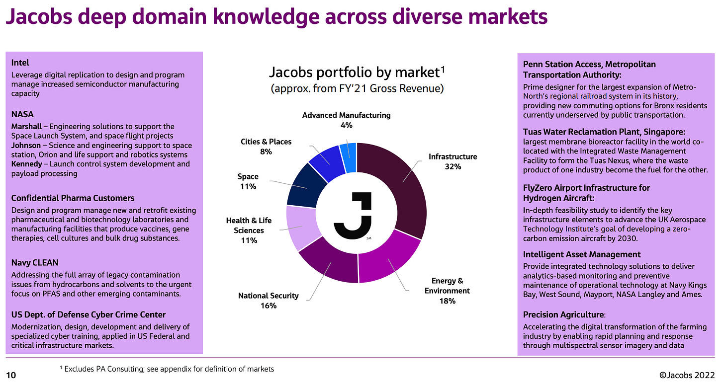
Jacobs is the number one engineering and construction services firm according to ENR with over $10 billion in annual revenue. While advanced manufacturing is only 4% of gross revenue they provide unique expertise through work with leading semiconductor manufacturers and technology partnerships.

Jacobs landed Intel’s new fab expansion in Arizona and “developed a design concept to match Intel’s next-generation manufacturing technology.” To manage this effort, Jacobs is using integrated production management software vPlanner, which is developed by firm owned by Ghafari, and building information modeling (BIM) design content replication methods.
Beyond semiconductors, Jacobs has developed “a dynamic management solution suite in Palantir Foundry that connects predictive AI modeling with day-to-day site operations to optimize power, chemical usage and asset management across plant sites” through a successful pilot that led to an extension of their strategic partnership.
Wood (Manufacturing)
Wood is a leading consulting and engineering companies operating across energy and materials markets. They leverage their expertise in facility automation, robotics and vision to drive innovation within automotive and electric vehicle battery materials.
Designing Europe's largest high-purity manganese processing facility
Wood will deliver front end engineering and design (FEED) and EPCm solutions for Europe’s largest proposed high-purity manganese processing facility as part of the Chvaletice Manganese Project, in the Czech Republic.
We have the mineral project capability and specialist expertise in advanced hydrometallurgy to successfully deliver this innovative project.
Integrating the first AI-based FeaturePrint™ for automotive manufacturing
Wood’s Machine Vision team out of Michigan is collaborating with a leading global automotive manufacturer, and software technology provider Alitheon, on an in-plant pilot for a cutting-edge AI-enabled vision system that will respond to the traceability challenge in automotive powertrain assembly.
They also have a years long partnership with Aspen Technology for “asset performance management (APM) technology for predictive and prescriptive maintenance.”
Ghafari Associates (Operations + Systems Engineering)
Ghafari is a global architecture, engineering, and consulting firm headquartered right next to the Motor City. It is no surprise that Ghafari’s expertise in the automotive industry is helping them lead the way in North America’s battery factory boom with four major electric vehicle battery facility projects:
BlueOval SK Battery Park in Glendale, Kentucky and BlueOval City in Stanton, Tennessee (Ford + SK On)
Ultium Cells Manufacturing Plant in Lansing, Michigan (General Motors + LG Energy Solution)
LG Lithium-Ion Battery Manufacturing Campus in Holland, Michigan (LG Energy Solution)
Ghafari also develops the vPlanner software through their in-house lean management consultancy. The vPlanner suite includes Takt planning, advanced Last Planner System® (LPS) implementations, Integrated Project Delivery (IPD) management, design for fabrication, and Target Value Delivery.
Exyte (Semiconductors)
As a dedicated partner of our clients, Excyte delivers semiconductor fabs from consulting and engineering through construction (management) to the hook-up of tools. We set the pace for the next generation of wafer fab design, built to meet our clients’ challenging technology roadmaps and precise economic targets.
Other Notable Firms
🔋 Batteries - Gresham Smith, SSOE Group, Wunderlich-Malec
💻 Semiconductors - Wunderlich-Malec
⚗️ Chemical - BSI Engineering, Matrix Technologies
Constructing the Factory 🏭🏗️
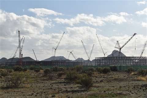
The construction of new factories also increases the need for more sustainable construction materials and advanced construction equipment. Steel maker Nucor has partnered with startup Electra to produce carbon-free iron that can be used to make steel. Holcim, the world’s leading cement producer, developed ECOPact a low-carbon concrete. Construction equipment is becoming smart with AI. Turner Construction is turning cranes into smart devices with the use of Versatile’s CraneView™ system. Caterpillar has deployed autonomous trucks to haul aggregates from quarry sites.

Planning for Factory Automation
Once the construction of a factory is complete, the next phase involves the installation of manufacturing equipment. This equipment is often selected with the help of the facility designers to best set-up the production processes that the facility was designed to house. The technology behind this equipment is a fascinating topic in its own right, encompassing everything from robotics and automation to data analytics and machine learning that is covered weekly in our Sunday digest. It’s what’s inside the factory, both skilled workers and automation, that makes a high-tech factory a high-tech factory.


